
Note: Please check your Spam or Junk folder, in case you didn't receive the email with verification code.
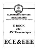
SYLLABUS
UNIT-1
Review of Semiconductors: Intrinsic semiconductors, Doped Semiconductors, Current Flow in Semiconductors, PN Junction with Open Circuit, PN Junction with Applied Voltage, Capacitive Effects in PN Junction. Diodes: Introduction, The Ideal Diode – current voltage characteristic, rectifier, diode logic gates, Terminal Characteristics of Junction Diodes– forward bias,reversebias, and breakdown regions, Modeling the Diode Forward Characteristics- exponential model, graphical analysis and Iterative analysis using the exponential model, constant voltage drop model, the small signal model.
UNIT-2
Diode Applications, Special Diodes: Zener diode Characteristics, Voltage shunt regulator, Temperature Effects, Rectifier Circuits– half-wave, full-wave and bridge rectifier circuits, rectifier with a filter capacitor, C-L-C filter, Clipping and Clamping Circuits– limiter circuit, the clamped capacitor, voltage doubler, Special Diode Types– UJT, Schottky barrier diode, Varactor diode, photo diode, Light Emitting Diode (LED), Problem Solving. Bipolar Junction Transistors (BJTs): Physical Operation - simplified structure and modes of operation, Operation of the npn, and pnp transistors: cutoff, active, and saturation modes, V-I Characteristics- of different configurations - graphical representation of transistor characteristics, dependence of collector current on collector voltage, the Early Effect.
UNIT-3
Bipolar junction Transistors: BJT circuits at DC,Applying the BJT in Amplifier Design- Voltage Amplifier,Voltage Transfer Characteristic (VTC), Small-Signal Voltage Gain, determining the VTC by Graphical Analysis, Qpoint, Smallsignal operation and models- the transconductance, input resistance at the base, input resistance at the emitter, Voltage gain, separating the Signal and the DC Quantities, The Hybrid-p Model, the T Model, Basic BJT Amplifier Configurations - Common-Emitter (CE) amplifier without and with emitter resistance, Common-Base (CB) amplifier, Common-Collector (CC) amplifier or Emitter Follower, Biasing in BJT Amplifier Circuits- Fixed bias, Self bias, voltage divider bias circuits, biasing using a Constant-Current Source,CE amplifier – Small signal analysis and design,Transistor breakdown and Temperature Effects, Problem solving.
UNIT-4
MOS Field-Effect Transistors (MOSFETs):Introduction, Device Structure and Physical Operation – device structure, operation with zero gate voltage, creating a channel for current flow, operation for different drain to source voltages, the P-channel MOSFET,CMOS, V-I characteristics – iD - vDS characteristics, iD – vGS characteristics, finite output resistance in saturation, characteristics of the p- Channel MOSFET, MOSFET Circuits at DC, Applying the MOSFET in Amplifier Design – voltage transfer characteristics, biasing the MOSFET to obtain linear amplification, the small signal voltage gain, graphical analysis, the Q-point. Problem solving.
UNIT-5
MOSFET Small Signal Operation Models: The dc bias, separating the DC analysis and the signal analysis, Small signal equivalent circuit models, the transconductance, the T equivalent circuit model, Basic MOSFET Amplifier Configurations – three basic configurations, characterizing amplifiers, common source (CS) amplifier without and with source resistance, common gate (CG) amplifier, source follower, the amplifier frequency response, Biasing in MOSFET Amplifier Circuits – biasing by fixing VGS with and without source resistance, biasing using drain to gate feedback resistor, biasing using constant current source, Common Source Amplifier using MOSFETs – Small signal analysis and design, Body Effect, Problem Solving.
 No Preview is available for this book

 Get 100 instant uPoints on the purchase of Rs.100 or above for each order.
CategoriesElectronics & Communication

Format PDF

TypeeBook